“A focus on scaling right from day one”
The TU spin-off NanoWired is ready to make its breakthrough on the market
2021/01/20
Products made by NanoWired GmbH – a recent “winner” at the Falling Walls conference – can be used in anything that requires connections from PCs, mobile devices, televisions or cars through to heart catheters and washing machines. For this purpose, the start-up – which was founded in 2017 – relies on conductive metal wires measuring just a few nanometres. Managing Director Olav Birlem explains why the company’s technology is so successful and how it will grow on the market. The electrical engineer and consultant is optimistic about the future despite the coronavirus pandemic.
TU Darmstadt: Mr. Birlem, a quick question at the beginning: How does NanoWiring work?
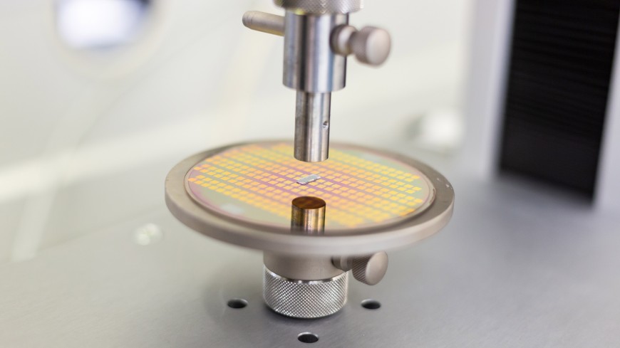
Olav Birlem: This technology is based on nanowires made out of copper, gold, silver, nickel, tin, zinc, indium and platinum. We use these wires to develop structures that can be attached to different surfaces like a metallic lawn. If you press these surfaces together, the nanowires become interwoven and create an extremely strong connection that is electrically conductive. This type of connection is comparable to a “klett” connection.
What special potential does this invention offer?
In theory, our “klett connections” could replace all standard connection technologies such as soldering, welding, screwing or bonding. NanoWiring is suitable for mechanical, thermal and electronic connections. One day in the future, all of us may carry this technology with us or even in us – e.g. in biosensor devices such as heart catheters or hearing aids. The diverse range of applications for our technology is part of our success story but we are of course still a long way from turning this vision into reality.
One day in the future, all of us may carry this technology with us or even in us – e.g. in biosensor devices such as heart catheters or hearing aids.
What is your short-term aim?
We are currently focussing on the electrical engineering sector because this is the area that we know best. For example, if you no longer have to solder the components on a circuit board for a computer, you consume less electricity and resources, save time and space and also generate less heat – meaning that the overall process is more resource and environmentally friendly.
Your first customer comes from the e-mobility sector. What is your selling point?
We want to launch products on the market that offer benefits to the whole of society. However, we need to think in rigid economic categories in order to achieve this. It is not enough for environmental technology to simply be cool. In particular, we highlight the added economic value that our products offer our customers, i.e. the ability for them to manufacture powerful devices while significantly reducing their energy footprint during production.
What is your business model?
We offer individual services and products, as well as an all-in-one package. This means that we sell engineering services, handle the production of small batches of products here at our premises and also offer the necessary hardware – NanoWiring machines and our Klettwelding tape. We have produced around 20 kilometres of this tape up to now. Customers can decide for themselves what it is that they require and how to integrate it into their production process.
You quickly cut the umbilical cord to TU Darmstadt, formed a GmBH in 2017 and have invested a lot of money in infrastructure. How is NanoWired financed?
Naturally, we have benefited from public funding programmes such as EXIST Transfer of Research or the LOEWE programme from the State of Hesse. I cannot stress enough how important this funding has been to us. However, we also won prizes such as the Venture Cup from Science4Life or the Hermes Award that have been invaluable during the start-up phase. The company has also secured two investors for the production infrastructure. Our financing model is currently based on three pillars. The investors pay for the infrastructure, we finance our machines from the funding programmes and aim to reinvest the money we earn from customers in the further development of the technology.
How do you plan to make your breakthrough on the market?
We have to break into the mass production market. This requires us to keep prices low, which in turn is only possible if a large number of customers buy a lot of our products. I am confident that when the first companies see that our technology can be scaled up and used for industrial applications, we will be able to acquire new customers at an ever faster pace.
We have to break into the mass production market.
Will you be able to cope with the demand if the market really starts to boom?
Yes. The most important thing is for us to be in a position today to secure the growth of the company in the future. We aim to achieve this by not only by expanding our infrastructure but also by further developing our strategy, acquiring new skills and bringing people to the company who have a wealth of experience in those markets in which we want to be active in the future. Finally, we hope to make enough progress so that we can become completely self-financed at some stage in the future.
What is your recipe for success?
A focus on scaling right from day one, creativity, highly professional management and a high tempo. And it is important that we try to maintain this tempo – even during periods of crisis.
The interview was conducted by Dr. Jutta Witte
The technology behind it all
The founders of NanoWired – Sebastian Quednau, Farough Roustaie und Florian Weißenborn – developed NanoWiring in the Institute of Microtechnology at TU Darmstadt. It is used in three different processes: KlettWelding, KlettSintering and KlettGlueing. The KlettWelding process connects two substrates equipped with NanoWiring at room temperature. The KlettSintering process creates a connection on just one substrate equipped with NanoWiring at 170° C, while the KlettGlueing process creates connections on fragile components using an adhesive. KlettWelding tape can even be used to connect untreated substrates with one another.